


The current computer infrastructure is based primarily on semiconductors. This class of electronic devices emerged around the mid-20th century and has seen capacity improvements at an almost exponential rate ever since. For decades, silicon has been the material used to make the transistors that power computer chips. The need to constantly increase performance, and reduce size, while maintaining low energy consumption has led to continuous miniaturization of transistors. The problem is that, like any material, silicon has physical limits beyond which the performance of the transistors degrades to the point of making them useless for their purpose, which is to act as a switch. IBM has used superconducting materials such as niobium and aluminum, patterned on a silicon substrate to make its quantum processors. And in 2022 it released the Osprey computer with 433 qubits — over three times the number of qubits of the 2021 Eagle computer. IBM tripled the number of qubits on a chip in just one year, and the famous computer manufacturer could soon release an even more powerful 1,000+ qubit machine. is suggest Big Blue is on track to deliver Condor, the world’s first universal quantum computer with more than 1,000 qubits, later this year.
But the power of quantum computers, and the kind of power needed to bring to fruition the artificial intelligence capabilities dreams (or nightmares) that, combined with AI, could be capable of generating new philosophical concepts. Now, the most important challenge in conductor electronics infrastructure is to increase the bandwidth of data transmission, energy efficiency, and information security, which is the role that quantum computing intends to fulfill. But to make quantum computing more accessible and shift away from the prototype phase — of which there are a few around the world, including Canada’s Xanadu (which uses a unique photonic approach to be discussed separately) — new materials as well as new design approaches will be needed.
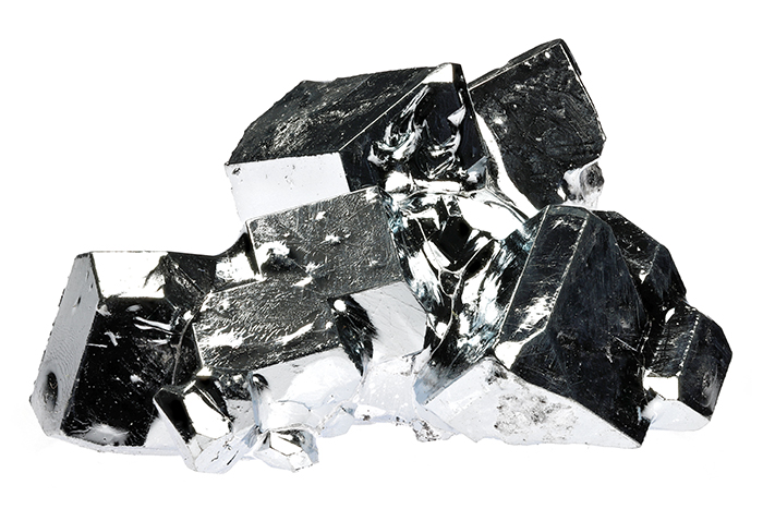
One of Those New Materials is Gallium Nitrate
Last March, the German Microchip manufacturer Infineon bet on the future by acquiring the Ottawa-Canada semiconductor manufacturer GaN Systems, paying US$ 830 million. Infineon’s CEO Jochen Hanebeck said that the company has taken this step to more readily expand its line of gallium nitride-based products. Semiconductors based on gallium nitride (GaN), rather than silicon, are increasingly in demand, and may eventually replace silicon altogether. GaN Systems is one of the top gallium-nitrate-focused companies in the world according to JPMorgan analyst Sandeep Deshpande. Efficient Power Conversion (EPC), NXP Semiconductors, and Wolfspeed are the others.
The fact that Infineon’s earnings per share will have been diluted by the almost $1B acquisition suggests that the German semiconductor manufacturer has faith in GaN’s continued growth and in the ability of gallium nitrate chips to threaten the supremacy of silicon ones. Silicon won’t be replaced entirely, as gallium nitrate will likely grow alongside a close relative of silicon: silicon carbide (SiC). Silicon carbide has been more popular until recently; because of its fewer defects per square centimeter, and it’s also easier to manufacture and achieve larger, and more uniform wafers of SiC than gallium nitride. But gallium nitride has proven to be more effective in smaller and higher frequency products, suggesting that if (or when) quantum computers reach the desktop stage, gallium nitride will present a distinct advantage. Infineon has been one of the leaders in SiC technology leaders.
Ultimately, whether silicon carbide or gallium nitride, the overall technological quest in quantum computer chips is to shift from semiconductors to superconductors. Superconductors allow electrical resistance to disappear as soon as they are cooled to a certain temperature. In order to find possible successors for today’s semiconductors, researchers — such as a group at Cornell University is doing — are studying heterostructures, i.e. structures made of two different types of materials. More specifically, they are looking for layered systems of superconducting and semiconducting materials because materials with very similar crystalline structures do not create tension in the crystal lattice at the contact surface according to John Wright, who produced the heterostructures for the new study at Cornell University. Gallium nitride, as you may have guessed by now, is one of these superconducting materials. The other is niobium nitride (NbN) The former has found increasing popularity in semiconductor electronics due to its now well-known characteristics. But to advance the technology and make it more ‘repeatable’, it is essential to understand how electrons behave on the contact surface of these two materials – and whether the semiconductors’ electrons cancel out the quantum effect by interfering with the superconductivity. Research using beamline spectroscopy at the Paul Scherrer Institute in Switzerland has shown that the electrons there are no unwanted interactions that could hinder quantum effects. The PSI scientists concluded that the superconductivity in NbN remains undisturbed, and that “a new form of semiconductor electronics that incorporates and exploits quantum effects in superconductors” is possible. Given the energy-saving but power-maximizing potential of the GaN, NbN, and other similar superconductivity designs, the evidence from PSI’s experiment should facilitate the advent of new microelectronics to support high data rates. This will not only make 5G (and 5+x G’s after that) faster but also faster charging – fast enough to make electric cars practical. Technological evolution will accelerate thanks to GaN, NbN, and other materials based on the former’s principles, eventually forcing silicon out of the Valley.


0 Comments